In this assignment, you will build a very simple micro-processor, that has a subset of instructions. The purpose of this assignment is to get familiar with verilog code and understand how to build a decoder, state machines. From assignment #4, you will build a graphics pipeline. The graphics pipeline also requires several pipeline stages to read instructions from memory/registers and ALUs just like assignment #3. So Assignment #3 will be provide a good foundation for the following assignments.
However, graphics pipeline needs many other units such as vector operations,
rasterization, VGA controllers etc, so the instruction sets in graphics pipeline will be more complicated. So do not try to optimize your verilog code.
The processor has only 4 instructions (Conditional branch, Add, LDW, SDW). The processor has 16-bit 8 registers and 256B Memory. The ISA is a fixed-length ISA and it has 16 bits.
You need to implement, BR, ADD, LDW and SDW. Architectural states, you need to implement PC, Registers, Memory, and 3-bit CC (NZP).
Requirements
There is no timing requirements for this assignment. However, you need to set up clock that does not have negative slack cycles. You could build 1-stage pipeline processor but I strongly recommend you to build a 5-stage like processor. Your graphics processor will also have several stages.
To simplify the problem, your processor can stall when there is a branch. We will only check the final outcome of values which will be written into memory.
You do not need to support unaligned memory accesses.
The initial PC value is 0x10. We use little endian.
Test Cases (All register values should be initialized with 0).
case1: assembly code , Binary assembly code MIF file , Output values
case2: assembly code , Binary assembly code MIF file , Output values
Please connect your register write signals to 7-Segment Displays. Your 7-Segment display should show your final data output.
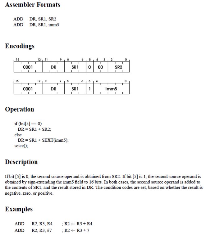
ADD
ADD DR, SR1, SR2
ADD DR, SR1, imm5


Operation
 if (bit[5] == 0) DR = SR1+SR2;
 else DR = SR1 + SEXT(imm5);
 setcc();
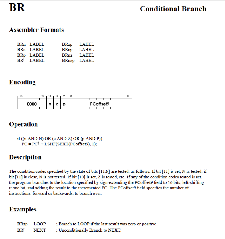
BRn Label
BRp Label
BRz Label
BRnzp Label

if (n And N) or (z and Z) or (p and P))
  pc = pc* + LSHF(SEXT(pcoffset9),1)

pc* is current pc+2;
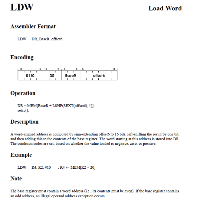
LDW DR, BaseR, offset

DR=MEM[BaseR+LSHR(SEXT(offset6),1];
Set cc();
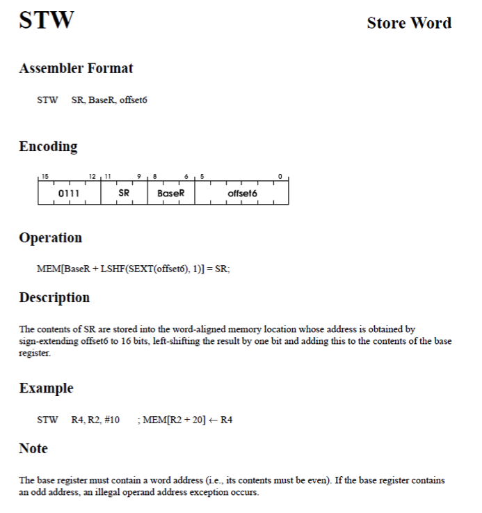
STW SR, BaseR, offset6

MEM[Base + LSHF(SEXT(offset6), 1)] = SR;
Initial PC value The program starts at 0x10. The instructions are a subset of LC3-B ISA.